Circuit Diagram Of Not Gate. It takes an input on the left and inverts it out on the right. Web january 16, 2022 by mir earlier we discussed the basic logic gates with truth table, circuit diagram and boolean expression.
Designing NOT Gate using Transistors from circuitdigest.com
Web 1 1 0 0 b 0 0 and is a boolean operation, an operation that takes values that are either true or false, and then outputs true or false based on a logical manipulation of those inputs. When applied +5v at base terminal, transistor start conduction. It can also be done using nor logic gates in the same way.
A Not Gate Performs Logical Negation On Its Input I.e If The Input Is True Or Logic 1, Then The Output Will Be False Or Logic Zero.
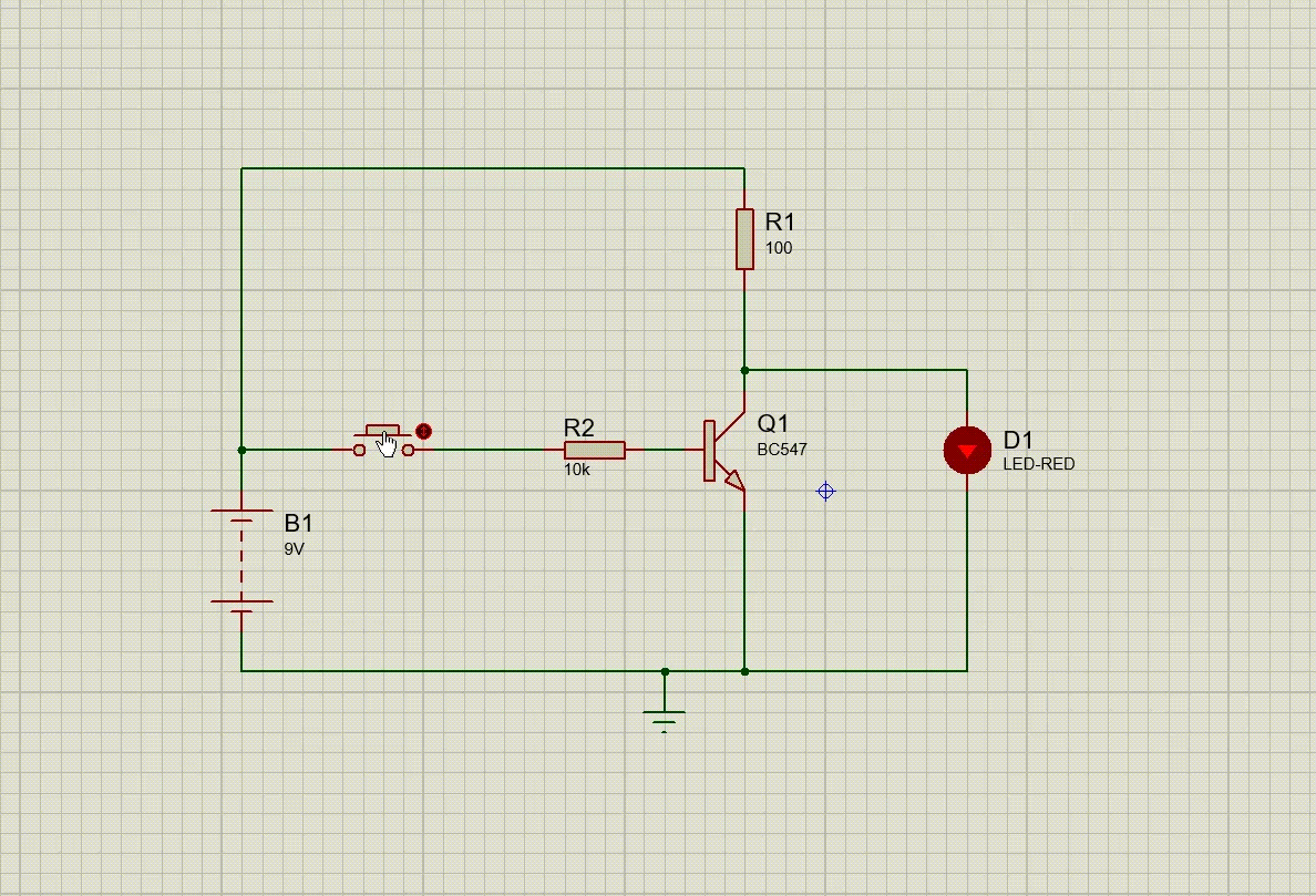
Web the circuit diagram of not with transistor is given below: Web the diagrams below show two ways that the nand logic gate can be configured to produce a not gate. Here, the transistor tx receives the required amount of potential to move into on condition.
It Takes An Input On The Left And Inverts It Out On The Right.
It can also be done using nor logic gates in the same way. Recall that a logic gate is a device that takes one or more binary inputs and has one binary output. The basic transistor circuit diagram is shown below.
Working Of Not Gate Let Us Understand The Working Of Not Gate With Transistor Circuit With High Input I.e.
Web the circuit diagram of a not gate using diodes is a classic example of how electricity can be used to construct an electronic logic gate. Web january 16, 2022 by mir earlier we discussed the basic logic gates with truth table, circuit diagram and boolean expression. The universal logic gates like nand gate and.
The Symbol Of The Not Gate Is A Triangle With A Bubble On Its End.
When the transistor moves into the on state, the voltage at b terminal will. It gives the complement of the input signal. A nor gate can be realized by using two bipolar junction transistors.
When High Voltage Is Applied As Input To The Inverter Which Is Vcc = +5V.
This is an incredibly important concept in modern integrated circuit design, as it forms the basis for many of the digital. When applied +5v at base terminal, transistor start conduction. This circuit was created by a member of the community and has no affiliation to the circuit diagram project.